
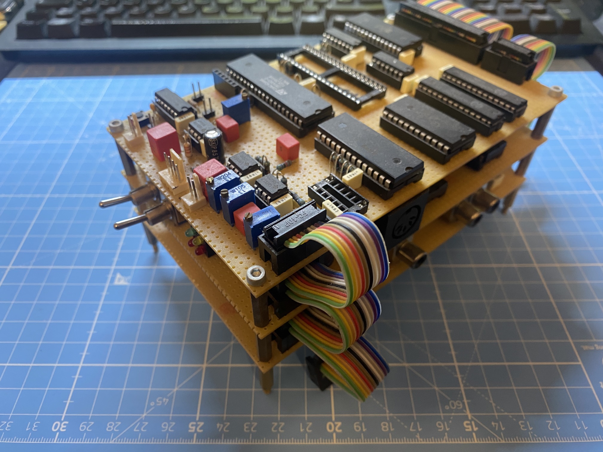
You might have already figured out that this isn’t my first attempt at designing and building a computer. There have been several prototypes along the way. The initial ones were built on breadboards, and the later ones on perfboard. The current version is the first with printed circuit boards. The previous iteration was already more advanced in terms of features.
It featured a working TMS9918 VDP and an AY3-8910 Sound Chip. After successfully implementing the console over the VDP, the next challenge was sound playback.
Since I haven’t written a tracker for my homebrew computer yet, the only way to play back music is by using PSG files. These files are essentially register dumps of the AY3-8910, and no tracker is required. The register states are sampeled at a fixed intervall and changed registers are dumped in the PSG file. The player then runs an ISR at the given interval and applies those changes to the registers of the AY3-8910. This is fairly easy to implement and works great by itself.
However, a notable issue arose – these files are inefficient in storing data. The maximum ROM size is 16KB. After subtracting the required space for the monitor and the playback program, there’s only enough room for a couple of seconds of audio.
While this was sufficient to prove that it works, it fell short of satisfaction.
Recognizing the need for improvement, I concluded that the next step would be to design and build a storage interface.
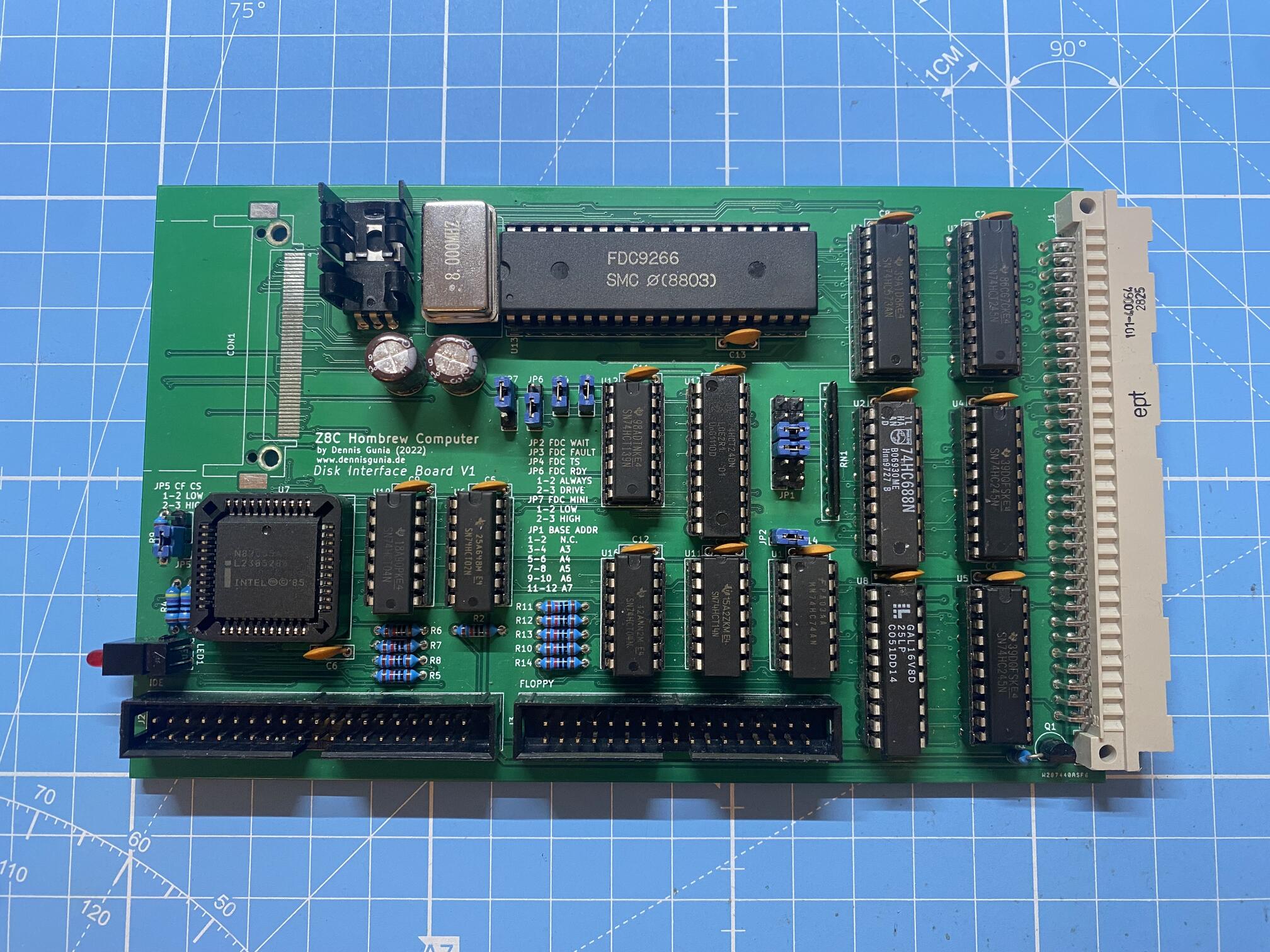
The Storage Interface Card
The new interface is already designed for my proprietary bus system. It features an IDE “Controller” and an FDC9266 floppy disk controller (FDC). The FDC is not yet tested. I am still lacking time on this project and have not yet been able to acquire a working 5,25″ floppy disk drive to test with.
I’m also still missing a CF-Card socket. The one I ordered had the wrong footprint so I had to order another one, hoping that this one finally has the correct footprint. Notice to myself: Order the parts before you design the PCB and make sure that it fits. It is free to change the footprint in KiCad, but it is expensive to manufacture another PCB or source hard to obtain parts.
What is working? Right now, the IDE interface is fully functional.
The IDE Protocol uses an 16-Bit bus to communicate with the controller. This is an issue since the Z80 only has an 8-Bit bus. Therefore I needed some logic to connect those two worlds. I searched a bit on the internet and came across several designs. Each one with its own pros and cons.
I opted to use the Intel 82C55A-2 Programmable Peripheral Interface IC to interface the IDE Bus.
The 82C55 is a very versatile chips. It connects to an 8-Bit bus. It is compatible with the Z80 timings and fast enough to still work at higher clock speeds of up to 8MHz without wait-states.
Designing an Interface around the 82C55 is very easy. There isn’t any logic involved. The IC only provides I/O to the IDE bus. The rest is done in software. This however makes the Interface slow and requires more CPU time. Also it does not allow DMA for reading and writing from disks which would be very helpful later on.
Interfacing the IDE Bus
As already mentioned, all IDE signals are controlled by the 82C55
Port A is directly connected to data-lines 0 thru 7.
Port B is directly connected to data-lines 8 thru 15.
Port C is connected to the remaining lines of the IDE bus.
Port C Pin 0-2 are connected to the Address Bus. Pin 3-7 are used for the control lines.
The 82C55 always operates in Mode 0!
You might have recognized that I “lied” earlier on. I mentioned, that we don`t need additional logic with the 82C55 but I have used inverters on some signal lines.
It is true, that you could connect them directly to the IO controller, however it makes it much easier to use if you invert the active-low signals using hardware.
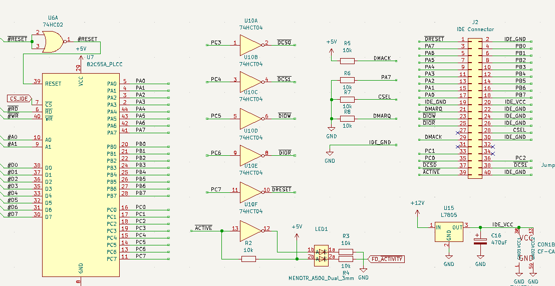
There is not much more to the hardware side of things. Some unused signals are pulled up or down and the activity line is connected to a buffer driving an indicator LED for disk access.
Software
I will not go into much detail on how to the IDE protocol works. There are many good resources out there. Here are some resources might prove helpful to you:
- http://blog.retroleum.co.uk/electronics-articles/an-8-bit-ide-interface/
- http://www.ardiehl.de/gide/
- http://www.gaby.de/gide/IDE-TCJ.txt
For low-level access I have built a “driver” to access the bus. It is the file “kdrv_ide8255.s” in the monitor rom. It provides the following functions:
ide_resetide_regwrite_8-> Write to 8-Bit registeride_regread_8-> Read from 8-Bit registeride_readsector_256-> Read 256 Words from IDE Bufferide_readsector_256_inv-> Read 256 Words from IDE Buffer but swap Bit 0-7 and 8-15ide_writesector_256-> Write 256 Words to IDE Buffer
The IDE-Driver can write to any location in the system memory.
With these basic functions, I have everything required to access IDE devices.
I’ve also already built a small device detector to find new disks:
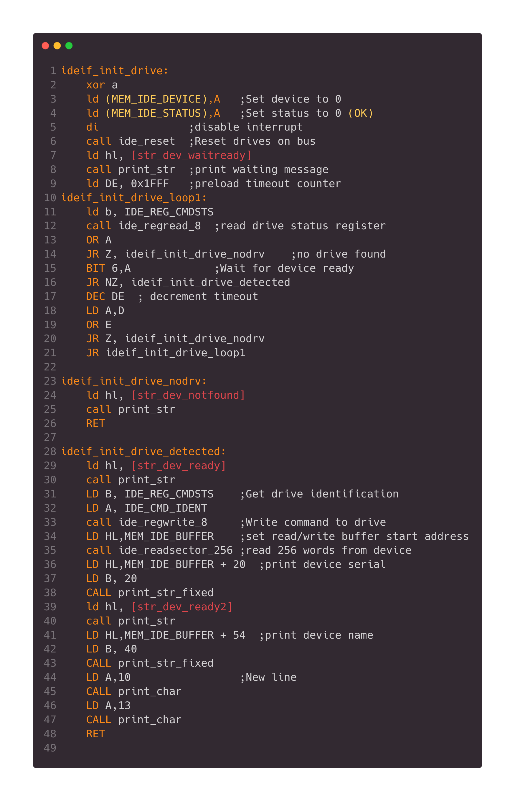
This detects a connected drive and prints it’s name and serial.
So far I’ve only tested it on CF-Cards. I might test it with real HDDs at some point.
Here is a screenshot using cool-retro-term running minicom serving as the terminal for my computer:
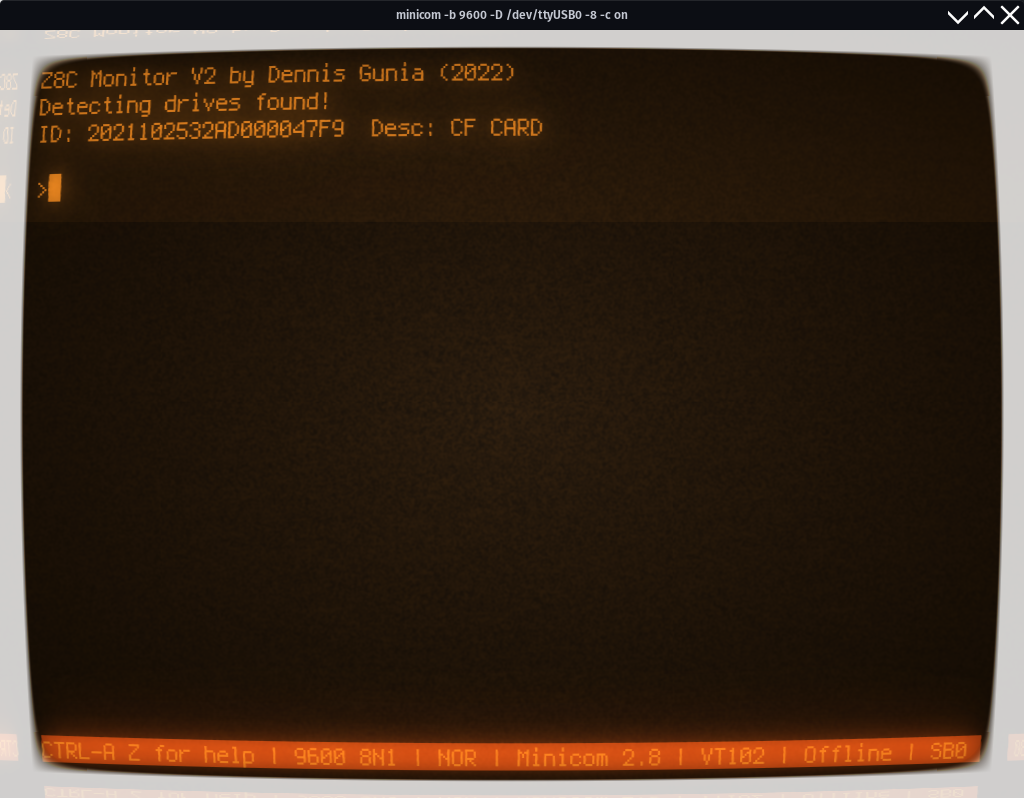
It detects the disk successfully and prints the name and serial.
Future plans
To fix the DMA and speed issues with my IDE controller, I plan to design and build a new one which allows faster transfer speeds, DMA and requires much less CPU time. I already have some ideas but as usual, not enough time.
Next step is to read out the MBR and detect partitions. Then implement some basic FAT16-routines. Read-only for the moment. I already made some progress there so stay tuned for some updates.
Complete schematics
https://github.com/dennis9819/Z8C-Homebrew-Computer/blob/master/Modules/001-CPU%20Board%20V1/Schematics.pdf